Electrostatic CRT Tester — Mark 2 · Volume 5
Electrostatic CRT Tester — Vol 5: The Build — Kits, PCB, Case & Jeff's Unit
Which kit tier to buy, what you actually solder, how the acrylic box goes together, wiring the banana panel — and the home of tjscientist's own build log
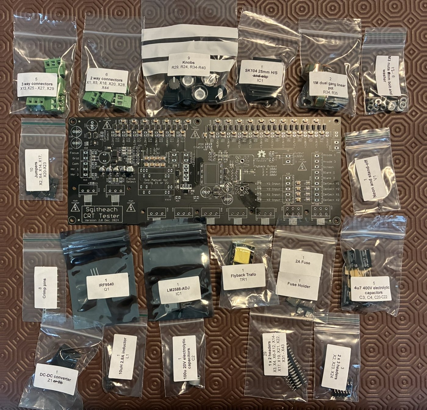
5.1 What this volume is (and what it defers)
Vol 4 traced what the board does — every supply from the 12 V barrel jack out to the banana panel, reasoned from the published specification because the detailed schematic and BOM live in the maker’s Dropbox rather than on the web pages. This volume is the other half of that story: how you turn a kit into a working instrument. Which tier to buy, what surface-mount work is (and isn’t) already done for you, the order you stuff and solder the through-hole parts, how the laser-cut acrylic case sandwiches together, and how you wire the 4 mm banana panel so that each jack lands on the right electrode.
It is also the home of Jeff’s own build log. Jeff has built one of these; the specifics — kit tier, case variant, build date, substitutions, tubes tested — aren’t in hand yet, so §9 is a skeleton awaiting his bench photographs and a fill-in details table. When the photos come in, that section becomes the record of this unit; until then it holds the shape of that record open.
Two honesty notes carried over from Vol 4, because they bound everything below:
- The full BOM and schematic are not public. The maker ships the complete-electronics kit with the through-hole parts bagged and labelled, and the detailed parts list lives in the Dropbox project folder — not on
crttester1a.html. So this volume does not quote resistor values, capacitor part numbers, or IC designators it has not seen. It reasons at the assembly level (component classes, mounting order, HV hygiene) which is exactly the level the labelled bags and the silkscreen put you at anyway. - The one part the maker names explicitly is the flyback transformer — the custom magnetic that makes kilovolts from 12 V. That is why it is the single component included even in the bare-bones £50 tier, and it is the marquee part of the build.
First power-up is deliberately brief here (§8) — the full bring-up sequence, in the correct order, with the metering, is Vol 6. This volume gets you to a powered board that hasn’t let its smoke out; Vol 6 brings a tube to life on it.
5.2 Choosing a kit tier
The maker sells the Mark 2 in three kit tiers plus build-to-order. They are not “good / better / best” — they are three genuinely different propositions aimed at three different builders, and picking wrong wastes either money or a weekend. Here they are with what each actually contains.
Table 1 — Choosing a kit tier
| Kit tier | Price (GBP) | What’s in the box | What you supply | Who it’s for |
|---|---|---|---|---|
| Minimum | £50 | Bare PCB + the flyback transformer only | Everything else — every R, C, semiconductor, connector, the hardware, the case | The well-stocked builder who wants only the two unobtainable items (board + custom magnetic) and will source the rest from stock |
| Electronics (complete) | £200 | PCB with all SMD parts pre-fitted, plus all through-hole parts and hardware in labelled bags, and the flyback | The 12 V supply, meters, HV probe, leads, and the case (unless you also buy a case kit) | The sweet spot — most builders. No fine-pitch soldering; just stuff, solder, and wire |
| Partial case | £100 | All case components except the laser-cut acrylic (3D-printed posts/handle/thumbscrews, M3 hardware, jacks, wire, heat-shrink) | The acrylic panels — cut from the maker’s provided files, or self-sourced | The builder who has (or can rent) laser-cutter access and wants to choose their own acrylic |
| Fully assembled & tested | On request | A finished, tested instrument | Nothing | The buyer who wants the tool, not the build |
A few things worth reading off that table:
- The £50 minimum tier is a component-sourcing exercise, not a discount. You are paying £50 for the two things you genuinely cannot make yourself — the PCB and the custom flyback — and taking on the job of finding every resistor, capacitor, semiconductor, connector, and mechanical part yourself against a BOM you’ll need from the Dropbox. For a builder with a deep parts drawer and time, it’s the cheapest route to the instrument. For anyone else it is a false economy: the £150 step up to the complete kit buys you all of those parts, correctly specified, pre-bagged, plus the SMD work done.
- The £200 complete tier is where the value is. The surface-mount parts — the fiddly ones, the fine-pitch ICs and 0805/0603 passives — arrive already reflowed onto the board (see §4). All you do is through-hole. That collapses the build from “source and place hundreds of parts, some of them tiny” to “fit the two dozen through-hole parts in the bags and solder them,” which is an evening’s work with an iron.
- Case is orthogonal to electronics. The case kit is a separate purchase from the electronics kit. The documented partial-case tier (£100) includes all the case hardware except the laser-cut acrylic, so it only makes sense if you can cut or source the acrylic yourself from the maker’s provided files. If you can’t, you’ll need to buy or commission the acrylic panels separately — or ask the maker about a fully-cased/assembled unit, which is available on request. (Confirm exact case-kit options on the shop page; the site documents the partial-case kit explicitly.)
5.2.1 A decision tree
                        Do you want to BUILD it at all?
                                    │
                 ┌──────────────────┴───────────────────┐
                No                                      Yes
                 │                                        │
        ┌────────┴────────┐              Is your parts drawer deep, and do you
        │ Buy it FULLY    │              WANT to source a full BOM yourself?
        │ ASSEMBLED       │                           │
        │ (on request)    │            ┌──────────────┴───────────────┐
        └─────────────────┘           Yes                             No
                                        │                              │
                          ┌─────────────┴──────────┐     ┌─────────────┴─────────────┐
                          │ MINIMUM kit £50        │     │ COMPLETE electronics £200 │
                          │ (PCB + flyback only —  │     │ (SMD done, TH parts +     │
                          │  you source the rest)  │     │  hardware bagged)         │
                          └────────────────────────┘     └─────────────┬─────────────┘
                                                                       │
                                              And for the case, can you laser-cut acrylic?
                                                                       │
                                                     ┌─────────────────┴─────────────────┐
                                                    Yes                                   No
                                                     │                                    │
                                         ┌───────────┴──────────┐        ┌────────────────┴───────────┐
                                         │ PARTIAL CASE £100     │        │ Buy/commission the acrylic │
                                         │ (cut your own acrylic │        │ panels (or ask about an    │
                                         │  from the files)      │        │ assembled unit).           │
                                         └───────────────────────┘        └────────────────────────────┘
The rest of this volume assumes the complete electronics kit (£200) + a case kit, because that is the path most builders take and the one the assembly walkthrough is written against. If you went minimum-tier, everything here still applies — you just have a sourcing job in front of the soldering job, and you’ll want the Dropbox BOM open the whole time.
⚠ The BOM you need is not on the website. For any tier below “complete,” and for any repair or substitution on any tier, you need the detailed parts list from the maker’s Dropbox project folder (“CRT Projects / CRT Tester” and “Common Stuff”). The web pages give tiers, prices, and the specification — not part numbers. Don’t try to reverse-engineer the BOM from the silkscreen; ask the maker for Dropbox access, which comes with the open-source design.
5.3 What’s on the board
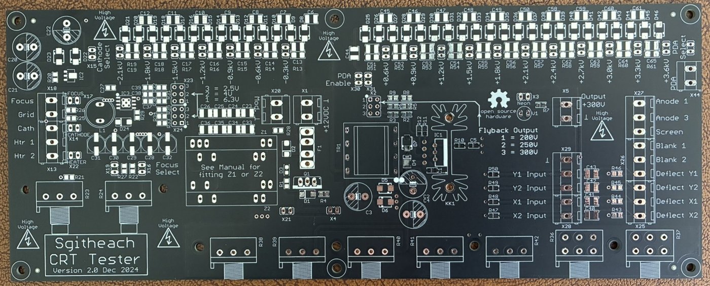
The Mark 2 is a mixed-technology board: surface-mount for the small, numerous, and fiddly parts, and through-hole for the large, high-voltage, mechanical, and user-serviceable parts. Understanding that split is the whole key to the build, because it tells you exactly what work the complete kit has taken off your plate.
Table 2 — What's on the board
| Part class | Technology | On the complete kit, who fits it? | Notes |
|---|---|---|---|
| Fine-pitch ICs, control/regulator silicon | SMD | Pre-fitted (reflowed at the factory) | The reason the complete kit needs no fine-pitch soldering |
| Small passives (biasing R/C, filtering) | SMD | Pre-fitted | 0603/0805-class parts you would not want to hand-place by the hundred |
| Large electrolytics, film/HV capacitors | Through-hole | You | Tall parts, fitted late (§5); HV film caps in the EHT/deflection sections |
| Power semiconductors, the switching devices | Through-hole (often heatsinked) | You | The flyback drive stage; may want a heatsink |
| The flyback transformer | Through-hole (custom magnetic) | You | The marquee part — see below |
| Potentiometers (BRIGHTNESS, FOCUS, a2, gains, positions) | Through-hole | You | The entire user interface — Vol 4’s “pots and jumpers” |
| Jumper headers / links (heater select, PDA select, meter) | Through-hole | You | Discrete selections per Vol 4’s controls map |
| Connectors — barrel jack, banana panel, wiring | Through-hole / panel | You | The board-to-world interface (§7) |
Read that as: the complete kit hands you a board that is electrically “done” for everything small and delicate, and leaves you the parts you’d want to place by hand anyway — the tall ones, the hot ones, the high-voltage ones, and the ones the user turns. That is a well-judged split. Nobody wants to reflow a fine-pitch regulator on a kitchen bench; everybody can solder a potentiometer and a transformer.
5.3.1 The flyback transformer — the marquee part
Vol 4 named the flyback as the key custom component — the one part with no distributor equivalent, wound to the maker’s design to make +2.2 kV (a2) and +5.6 kV (PDA) from 12 V through the multiplier ladder. In the build, it is the physical centrepiece:
- It is the one part included in every tier, even the £50 minimum — because it is the one part you can’t just order.
- It is a tall, heavy, through-hole part, so it gets fitted in the later mechanical passes of the build (§5), not with the low-lying components.
- Its secondary sits at the head of the EHT chain, so the PCB real estate around it is the highest-voltage region on the board. Everything about HV hygiene in §6 is most critical right here.
Treat the flyback as you would the mains transformer in a valve amp: mechanically the anchor of the board, electrically the origin of everything dangerous. Fit it square, seat it fully, solder its pins generously (they carry real current and take mechanical strain), and keep the region around its secondary clean.
5.4 Through-hole assembly walkthrough
The universal rule of hand assembly applies: fit the lowest-profile components first and work up in height, so the board always lies flat on the bench against the part you’re currently soldering. On top of that, this board has a high-voltage section that wants specific care. Here is the order.
Step 1 — Lowest components first. Any through-hole resistors, diodes, and small signal parts in the bags go down first: insert, splay the leads to hold them, flip the board flat onto the bench, solder, clip the leads. Working lowest-first means each subsequent taller part can’t stop the board sitting flat. (On the complete kit most of the small passives are already SMD and reflowed, so this pass is short — mostly the through-hole parts the design chose to keep serviceable.)
Step 2 — IC sockets / low semiconductors, jumper headers. Any DIP sockets, jumper/link headers (heater-select, PDA-select, meter-route — the discrete choices from Vol 4’s control map), and small transistors go next. Sockets before the parts that go in them. Get header rows square — a crooked jumper strip is a lifelong annoyance.
Step 3 — Potentiometers. The pots — BRIGHTNESS (grid bias), FOCUS, a2 ADJUST, the deflection gains and positions — are the user interface and they must end up square, aligned, and at a consistent height so the shafts pass cleanly through the acrylic front panel and the knobs sit level. Fit them, but consider tacking one pin, checking alignment against the panel (dry-fit the acrylic if you have it), then soldering fully. Their mechanical alignment matters more than any electrical part on the board because the case depends on it.
Step 4 — Capacitors, tall passives. Electrolytics and film/HV capacitors now — polarity-critical parts, so double-check band/stripe orientation against the silkscreen before soldering. The HV film caps in the EHT and deflection sections belong to the high-voltage region; note where they are, because §6’s hygiene rules apply to their pads.
Step 5 — Power semiconductors + heatsinking. The switching device(s) in the flyback drive stage, and anything else that dissipates, go on with their heatsinks. Torque any heatsink hardware before final soldering so you’re not stressing solder joints to seat a sink. Insulating washers/pads where the design calls for them.
Step 6 — The flyback transformer. The marquee part (§4.1). Seat it fully flat, square to the board, and solder its pins with enough fillet to carry current and take strain. This is the tallest, heaviest single part and the origin of the EHT — get it mechanically solid.
Step 7 — Connectors and the board-to-world interface. The 2.1 mm barrel jack, any board-edge connectors, and the wiring pigtails to the banana panel (§7) go last, because they’re the interface to the case and you want them fitted after everything they connect to is in place.
Step 8 — Inspect, then clean. Before power (Vol 6), inspect every joint under magnification, then clean the flux off — which for this board is not cosmetic but a safety step, per §6.
5.4.1 HV-layout hygiene — the callout that matters most
Most of that walkthrough is generic good practice. This part is specific to a board that runs at kilovolts, and getting it wrong doesn’t cost you a re-solder — it costs you tracking, corona, arc-over, and eventually a dead board or a shock.
⚠ High-voltage assembly hygiene — the EHT section is not an ordinary board. Around the flyback secondary, the multiplier ladder, and the a2/PDA/deflection nodes, the board sits at hundreds to thousands of volts. At those potentials three things bite you that never matter on a 5 V logic board:
- Flux tracks at kV. Rosin/no-clean flux residue is mildly conductive and it will happily carry leakage current — or strike into a carbonised track — across a high-voltage gap. Clean all flux off the EHT region thoroughly (isopropyl + brush, or an ultrasonic bath if the parts allow) so those pads are bone-dry and residue-free. This is why §5 ends with “then clean” as a safety step.
- Sharp solder points emit corona. A spiky, unsmoothed solder joint or a snipped lead-end left as a point is a field concentrator — it will corona (ionise the air around it) at high voltage, wasting energy, making ozone, and starting the erosion that leads to a flashover. Dress every HV joint smooth and rounded; clip leads flush and, ideally, dab the cut end. No sharp points anywhere the voltage is high.
- Creepage and clearance are sacred. The designer set the copper spacing (clearance through air) and the surface distance around slots (creepage) for the working voltage. Don’t bridge them — no stray solder blobs across an EHT gap, no wicking a whole node together, no “helpful” extra wire that shortens a gap. If a slot is cut in the board between HV nodes, it’s there to lengthen the creepage path; keep it clean and unbridged.
The failure mode isn’t subtle once it starts: a faint blue glow or hiss around a point at power-up, a smell of ozone, or a fine carbonised line growing across a dirty gap. If you see or smell any of that, power down and clean/dress the offending spot before continuing. Full HV safety discipline — bleeding nodes, one-hand rule, EHT-rated leads — is Vol 8; this callout is specifically about building the HV section so it doesn’t bite you later.
5.5 The case
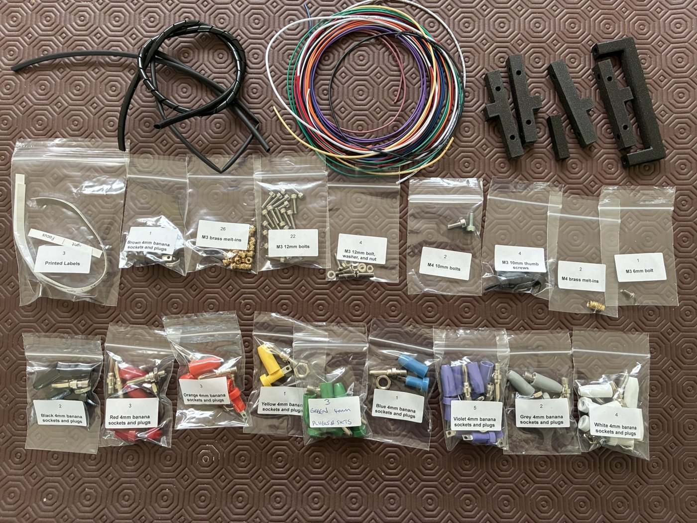
The Mark 2 lives in an open, laser-cut acrylic box — a deliberate design choice that suits an instrument you watch working (you can see the flyback, the wiring, and the glow of the tube under test) and that puts the banana panel and pots where your hands go. The construction is a clear-acrylic sandwich held on 3D-printed corner posts.
5.5.1 Case bill of materials
Table 3 — Case bill of materials
| Item | Spec | Role | In partial-case kit (£100)? |
|---|---|---|---|
| Laser-cut acrylic panels | 5 mm or 6.35 mm clear acrylic | Top/bottom/sides + front (jack/pot) panel | No — you cut these from the provided files |
| Corner posts | 3D-printed | Stand the panels off each other; the structural skeleton | Yes |
| Handle | 3D-printed | Carry the instrument | Yes |
| Corner thumb screws | 3D-printed | Tool-free panel fastening at the corners | Yes |
| Machine screws / standoffs | M3 hardware | Fasten panels, mount the PCB | Yes |
| Banana jacks | 4 mm | The electrode panel (§7) | Yes |
| DC input jack | 2.1 mm barrel | 12 V input | Yes |
| Hook-up wire | assorted | Board-to-panel wiring | Yes |
| Heat-shrink | assorted | Insulate the HV panel wiring | Yes |
The acrylic thickness choice (5 mm vs 6.35 mm) is the one case decision worth thinking about: 6.35 mm (¼ inch, the common US acrylic stock) is stiffer and more implosion-forgiving if you’re ever handling a tube close to the box; 5 mm is lighter and the common metric stock. The provided cutting files are dimensioned for the maker’s build — if you cut your own on the partial-case tier, cut for the thickness the files specify, or adjust the slot/tab geometry to your stock.
Note — acrylic cutting files are provided (Dropbox). The partial-case builder cuts their own panels from these files. They’re vector cut files (the same open-source release as the electronics), so any laser cutter or a cutting service can run them. If you’re sourcing your own acrylic, match the file’s thickness or you’ll have tab/slot fit problems in the sandwich.
5.5.2 Case assembly order
The case goes together in an order dictated by access — you wire what you can’t reach later, first.
  1. WIRE THE JACK/FRONT PANEL first (while it's loose and reachable)
        ├─ mount 4 mm banana jacks + 2.1 mm DC jack into the front acrylic
        ├─ mount the pots' shafts through the panel (or board-mounted pots
        │  poke through — depends on your pot mounting)
        └─ run the board-to-jack wiring, heat-shrink every HV run (§7)
                                │
  2. MOUNT THE PCB to its acrylic base panel on M3 standoffs
        └─ board sits on standoffs so nothing on the underside shorts to a panel
                                │
  3. STAND UP THE CORNER POSTS (3D-printed) on the base
                                │
  4. CLOSE THE ACRYLIC SANDWICH — side/top panels onto the posts
        └─ peel the protective film off the acrylic BEFORE final assembly
                                │
  5. FIT THE 3D-PRINTED CORNER THUMB SCREWS + the HANDLE
        └─ tool-free thumb screws mean you can reopen it to service/probe
Two practical notes. First, peel the acrylic’s protective film before you close the box, not after — it’s maddening to reach a film edge through an assembled sandwich, and any film left on is a place for the panel to look permanently “foggy.” Second, wire the panel before you mount the board where you can — the whole point of the open sandwich is access, but the jack-panel HV wiring is far easier to run and heat-shrink with the panel in your hand than buried in a closed box.
For a reference of what the finished, cased instrument should look like, see the assembled unit below and cross-check your panel layout against it.
5.6 Wiring the banana-jack panel
This is the step that turns a powered board into a usable tester: every electrode a CRT needs is brought out to a 4 mm banana jack on the panel, so you can patch the tube to the instrument with banana-to-flying-lead cables. The mapping follows directly from Vol 4’s block diagram — each jack is the terminus of one rail traced there.
The maker doesn’t publish a fixed panel silkscreen (Vol 4’s control map is design-reasoned), so the panel below is the functional set of connections the instrument must bring out, grouped by the electron-gun order from Vol 2 / Vol 4. Confirm the exact silkscreen against your board.
Table 4 — Wiring the banana-jack panel
| Panel jack | Rail it lands on (see Vol 4) | Voltage class | Suggested colour |
|---|---|---|---|
| Heater ×2 | Heater converter output, ≤6 W (2.5–6.3 V) | Low | Brown / brown |
| Cathode (k) / common return | Cathode-return reference — the node everything is measured against | Reference (0 V ref) | Black |
| Grid g1 | Negative bias rail via BRIGHTNESS pot (−5 to −120 V) | Medium (−V) | Orange |
| Focus a1 | Focus divider off a2 (hundreds of V to ~1 kV) | HV | Yellow |
| Accel a2 | a2 tap on the EHT ladder (up to +2.2 kV) | EHT — lethal | Red |
| PDA | Top-of-ladder PDA tap (up to +5.6 kV) | EHT — lethal | Red |
| X1 / X2 | Horizontal deflection plates, push-pull (±300 V) | Medium-HV | Blue / blue |
| Y1 / Y2 | Vertical deflection plates, push-pull (±300 V) | Medium-HV | Green / green |
| Z (grid modulation) | AC-coupled modulation onto g1 | Signal | White |
| Meter tap(s) | External I / V meter routing (Vol 4 metering) | per node | Grey |
A few wiring principles for this panel specifically:
- Colour-code by hazard, not just by function. The single most useful convention is to make a2 and PDA visually unmistakable — red, and ideally physically separated on the panel — because those are the jacks that will hurt you and the ones you patch last and unpatch first. Vol 6’s bring-up order (a2 up first, PDA up last) maps onto the panel’s physical layout if you group the EHT jacks together and apart.
- Heat-shrink every HV run behind the panel. The wiring from the board to the a2, PDA, focus, and deflection jacks sits at hundreds to thousands of volts inside the box. Use wire rated for the voltage, keep the runs short and dressed, and heat-shrink the jack terminations so there’s no bare HV metal loose in the box (this is what the heat-shrink in the case kit is for).
- Cathode is the reference — treat it as such. The cathode/common jack is the node Vol 4’s whole architecture is defined against. Wire it solidly; it carries the beam-current return that the metering (Vol 4 §metering) reads.
- Keep the deflection pairs paired. X1/X2 and Y1/Y2 are differential; run each pair together and keep them straight to the plates so the push-pull balance Vol 4 describes actually reaches the tube balanced.
Cross-ref — Vol 4 block diagram. Every jack in the table above is the output end of one rail in Vol 4’s functional block diagram and signal-flow summary. If a connection here is unclear, follow the rail back through Vol 4 (e.g. “why is focus derived from a2?” → Vol 4 §focus supply, and note that re-touching focus after any a2 change is expected).
5.7 First power-up — the smoke test
This is the brief version. The full bring-up sequence — heater first, then bias, then accel, then focus, then deflection, then PDA last, each with its metering — is Vol 6. What follows is only the “did I build it right?” check you do before any tube is anywhere near the instrument.
  SMOKE-TEST SEQUENCE  (NO TUBE CONNECTED)
  ───────────────────────────────────────────────────────────
  1. Bench supply set to 12 V, CURRENT-LIMITED to a low value
     (a few hundred mA over expected idle). A current limit is
     your smoke insurance — a build fault trips the limit instead
     of cooking a part.
  2. Power on. Watch the supply's current reading.
        • Sane idle current, no smoke, no smell  → good, continue.
        • Current slams to the limit / a part heats / smell → OFF.
          Find the fault (reversed cap, solder bridge, backwards
          semiconductor) before trying again.
  3. Check the low-voltage rails come up where expected
     (heater rail present at a heater setting, bias rail negative,
     logic/control rails per Vol 4).
  4. VERIFY EHT IS PRESENT — with a kV-rated HV probe ONLY —
     on the a2 and PDA jacks. Confirm the flyback/multiplier is
     making high voltage BEFORE you ever connect a tube.
  5. BLEED the a2 and PDA nodes to the cathode-return with an
     EHT-rated bleeder before touching anything. The multiplier
     holds kV after power-off (Vol 4 §stored-charge).
  ───────────────────────────────────────────────────────────
  Only after this passes do you go to Vol 6 and bring up a tube.
The current-limited-supply habit is worth stating plainly: set a current limit on the 12 V supply and the worst a build fault can do is trip the limit. Every reversed electrolytic, solder bridge, or backwards transistor announces itself as the limit light coming on instead of a part venting. It is the cheapest insurance on the bench.
⚠ EHT is lethal — this is not a low-voltage board. The moment step 4 succeeds, this instrument has up to +5.6 kV (PDA) and +2.2 kV (a2) on its panel and, critically, stored in its multiplier capacitors after you switch off. Verify EHT only with a proper kV-rated HV probe — never an ordinary DMM hung directly on the jack. Bleed every EHT node to the cathode-return before you reach into the box, and follow the one-hand rule above ~50 V. The full safety discipline — bleeding, EHT-rated leads, CRT implosion and X-ray hazards, the ±300 V and −120 V shock hazards — is Vol 8. Do not bring a tube up (Vol 6) until you have both verified EHT is present and proven to yourself you can bleed it down.
5.8 Jeff’s build log — tjscientist’s unit
This section records one built Mark 2. The build details below are confirmed; bench photographs are still to come.
5.8.1 Build details
Table 5 — Build details
| Field | Value |
|---|---|
| Kit tier built | Complete electronics kit (£200) — PCB with all SMD parts pre-fitted, through-hole components + hardware supplied bagged. No fine-pitch hand-soldering required; the through-hole stuffing + the flyback are the build. |
| Case | Custom — self-cut on Jeff’s own laser cutter (his own design/panels, not the maker’s supplied acrylic). Material gauge and layout: from Jeff’s photos. |
| Custom additions | Custom tube-socket holders — Jeff’s own fixtures for mounting/adapting the CRT and valve sockets to the tester, beyond the stock banana-lead connection. A distinctive personalisation of this unit; a photograph is pending. |
| Build date | TBD — from Jeff (ISO YYYY-MM-DD) |
| Deviations from docs | Case + fixturing only — self-designed laser-cut enclosure and custom socket holders in place of the stock case/lead scheme; electronics per the maker’s kit. |
| Parts substituted | None noted — complete electronics kit built as supplied. |
| Tubes tested so far | TBD — from Jeff (which CRTs / neon / magic-eye devices, with any measured results worth logging) |
| Serial / provenance | TBD — from Jeff (if the maker numbered the unit — for MY_GEAR) |
Two things make Jeff’s unit its own: a self-laser-cut case rather than the maker’s acrylic panels (the design is fully open, so cutting your own from your own files is squarely in the spirit of the project — see Vol 3), and a set of custom tube-socket holders that turn the tester from a banana-lead-per-electrode rig into something you can seat a tube into more directly. The socket holders are the more interesting engineering touch: the stock tester brings each electrode out to a 4 mm jack (Vol 4 §control map, and §7 here), so a holder that lands a real tube base’s pins onto those electrode nodes — while keeping the HV pins properly spaced and creepage-safe (mind the §5.1 HV-hygiene rules at the socket, where a2/PDA can sit at kV) — is exactly the kind of fixture that makes repeated CRT testing quick and repeatable.
5.8.2 The build, in photos
5.8.3 Notes to fill from the build
When the details come in, this space captures the specifics that don’t fit the table — the engineer’s-logbook narrative:
- Kit-tier rationale — why this tier (deep parts drawer → minimum? no fine-pitch appetite → complete?), and how the actual build compared to §2’s expectations.
- HV-section notes — how the EHT region cleaned up, any corona/tracking seen on first power-up (§6), and how it was dressed.
- Smoke-test result — the idle current at 12 V, whether EHT came up first try (§8), and the measured a2/PDA levels on the HV probe.
- Panel wiring choices — the actual colour-code used (§7), and any deviations from the suggested map.
- First tubes — the first CRT (or neon/magic-eye device) brought up on it, cross-referenced into Vol 6 (the CRT-under-test photo) and Vol 7 (the device menagerie).
Vol 5 built the box. Vol 6 brings a tube up on it — the full, ordered power-up sequence (heater → bias → accel → focus → deflection → PDA), the metering procedures, and reading gun faults off the meters. Vol 8 is the complete HV / CRT safety discipline this volume’s callouts point at.
Comments (0)